ALBA Synchrotron
Researchers have demonstrated that bending tiny ferromagnetic nanowires — introducing curvature — allows precise control over special three-dimensional magnetic textures called "Bloch point domain walls" (BPDWs). Straight sections of the wire naturally pin these magnetic walls, while curved parts change their stability and motion, enabling the ability to pin or move them simply by shaping the wire.
For the first time, researchers have experimentally shown that bending nanowires creates asymmetric energy traps that control how Bloch points domain walls move — and that their motion depends on direction. This curvature-induced symmetry breaking reveals how both the central magnetic singularity and its surrounding texture contribute to pinning. The study also introduces the idea of a “Bloch point shift register” — a device controlled purely by the wire’s shape, demonstrating that geometry alone can steer magnetic behavior at the nanoscale.
The study was led by Sandra Ruiz Gomez (currently working at the ALBA Synchrotron) and Claire Donnelly, both from Max Planck Institute for Chemical Physics of Solids, with collaborators from institutes across Europe, including ALBA, SOLARIS Synchrotron, University of Vienna among others.
Controlling Bloch point domain walls opens exciting possibilities for creating high-density, three-dimensional magnetic memory and logic devices that are more efficient and compact. Beyond magnetism, this approach of tuning magnetic behavior through wire shape could also apply to other advanced quantum materials, like superconductors and van der Waals magnets. Additionally, the research provides important insights into the fundamental physics of topological singularities, which are key to creating and controlling complex 3D magnetic structures such as skyrmions and hopfions — offering new directions for future technologies.
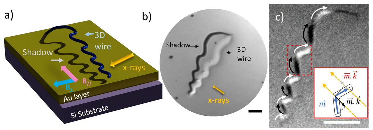
The research team used advanced 3D nanofabrication (focused electron beam induced deposition) to fabricate cobalt nanowires with alternating straight and curved segments. Using X-ray magnetic circular dichroism photoemission electron microscopy (XMCD-PEEM) at the CIRCE beamline of ALBA and at the DEMETER beamline of SOLARIS, they tracked the position and motion of BPDWs under applied magnetic fields. Micromagnetic simulations complemented the measurements, disentangling the effects of curvature on the surrounding magnetic texture from those of the Bloch point singularity itself. The experiments revealed that straight regions consistently pin BPDWs, and that varying curvature sets the height of nearby energy barriers, producing asymmetric potential wells and direction-dependent propagation fields.

d) XMCD image of the same structure after the nucleation of a domain wall applying magnetic field perpendicular to the long axis of the nanostructure. The position of domain wall is denoted with a red arrow. e) Zoom of the previous image in the region where the domain wall is located. f) Zoom of the same domain wall after rotating the sample (25o) to measure with the X-rays oriented perpendicular to the wire. Yellow arrows indicate the direction of the incoming beam. The sketch shows the projection of the magnetization with respect to the X-ray direction. g) XMCD image of the same structure after the nucleation of a domain wall applying a magnetic field parallel to the long axis of the nanostructure. The position of the domain wall is denoted with a red arrow. h) Zoom of the previous image in the region where the domain wall is located. i) Zoom of the same domain wall after rotating the sample to measure with the X-rays oriented perpendicular to the wire. Yellow arrows indicate the direction of the incoming beam. The sketch shows the projection of the magnetization with respect to the X-ray direction. The scale bar is 1 µm in all cases.